A logic level converter, also called a logic level shifter, is commonly used for voltage conversion when interfacing devices. In simple circuits, a voltage divider is often used to shift logic levels. But voltage dividers have high output resistance which makes them unsuitable for shifting voltages in some applications.
In this article, you will learn:
- Circuit and working of unidirectional logic level converter using transistor.
- Schematic and working of bidirectional logic level converter using MOSFET.
- Pinout details of a logic level converter breakout board.
What Are Logic Levels & Logic Families?
In digital electronics, a signal can be either ON or OFF. The ON state is called logical high(1) and the off state is logical low(0). Logic levels are a range of defined voltage states for which a signal can be termed as high or low.
For example in the case of TTL signal inputs (Transistor-Transistor logic), any voltage between 2V and 5V is considered logical high, and voltage in the range of 0V to 0.8V is considered logical low.
TTL, CMOS, LVCMOS, LVTTL, etc. are some examples of logic families that may use different threshold voltages to define logical high and logical low.
What is a Logic Level Converter?
A logic level converter or logic level shifter is a necessary circuit while interfacing devices with different voltage requirements. Logic level converter steps up or steps down the voltage as per the requirement of a device.
For example, if we want to send serial data from an Arduino UNO to an ESP32 development board, we need to use a logic level shifter as the output from the Arduino RX pin can output up to 5V while the TX pin in ESP32 can only tolerate 3.3V.
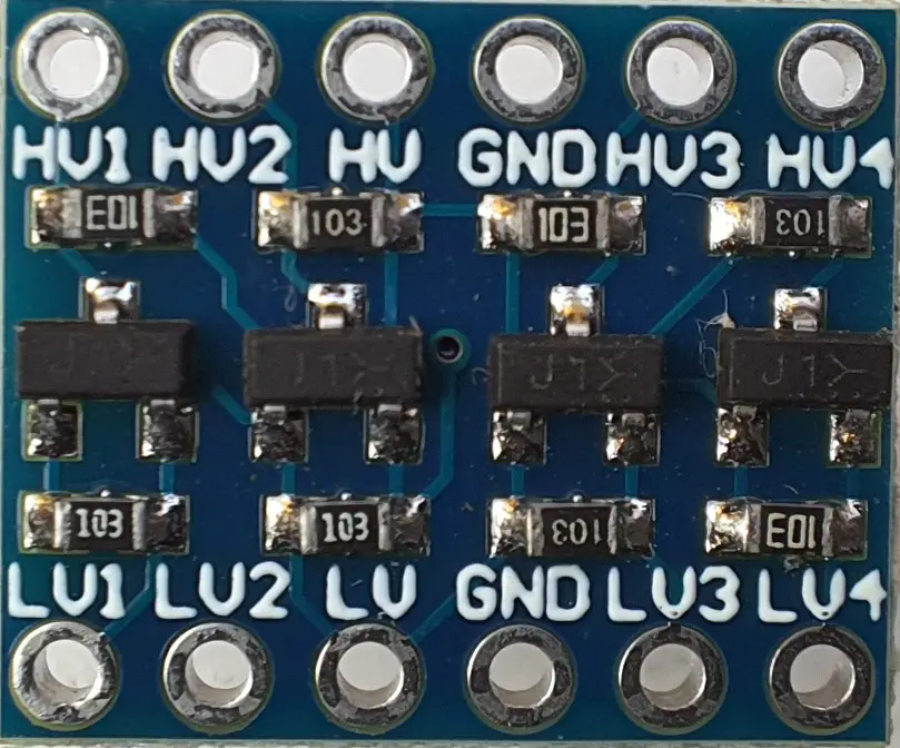
The image above is a commonly available bidirectional logic-level converter breakout board module, which will be described shortly in this article. A unidirectional level shifter can translate one voltage level to another, while a bidirectional logic level shifter facilitates the two-way conversion of voltage levels.
For example, to send data from a CMOS (5V) device to an LVTTL (3.3V) device, we can use a unidirectional level shifter that shifts 5V output to 3.3V. But for two-way data transfer between CMOS and LVTTL compatible devices, we require a bidirectional logic level converter that can also shift LVTTL output voltage to CMOS input voltage.
Logic Level Converter Circuit using a Transistor
A simple unidirectional logic level converter can be designed using a single NPN transistor and two resistors.
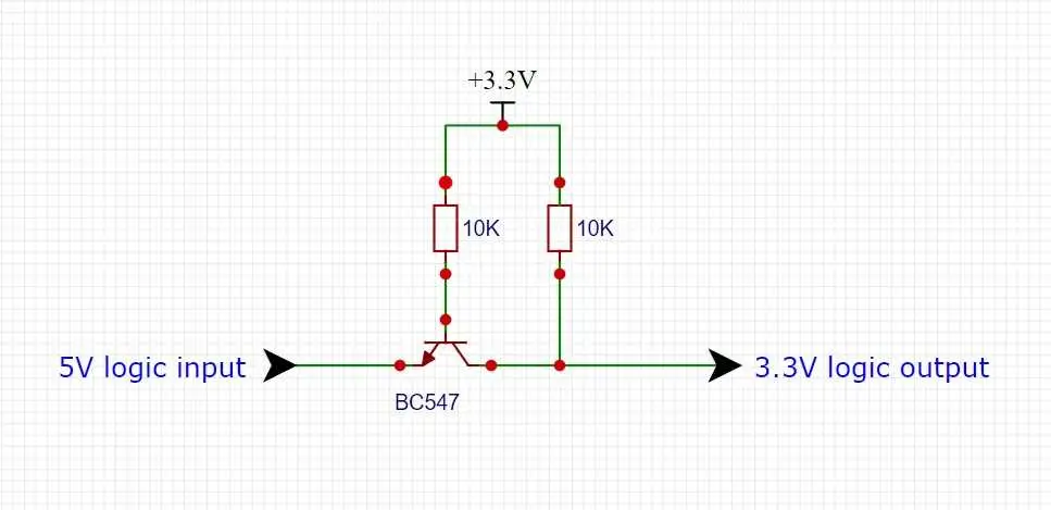
The circuit above can be used to convert 5V signals to 3.3V. The commonly used BC547 transistor can be chosen for this purpose. Note that the grounds of both voltage sources should be connected.
Consider the situation when the input to the emitter of the transistor (5V input pin) is at 0V. Then the transistor turns ON due to a potential difference of 3.3V between its base and emitter. Due to this the collector also gets pulled to the ground and we get 0V on the collector side of the transistor. Hence for 0V on the input, we get 0V output.
When the voltage at the input is at 5V, the transistor remains OFF and the collector is pulled to 3.3V by the 10K resistor. So for 5V at the input, we get 3.3V output.
Thus, the input and output voltage can be related as:
| Input Voltage | Output Voltage |
| 0 Volt | 0 Volt |
| 5 Volt | 3.3 Volt |

Bidirectional Logic Level Shifter using MOSFET
An n-channel MOSFET and two resistors can be used to make a bidirectional logic level converter. The positive of the high voltage supply should be connected to the HV node(D), and the low voltage supply should be connected to the LV node(C).
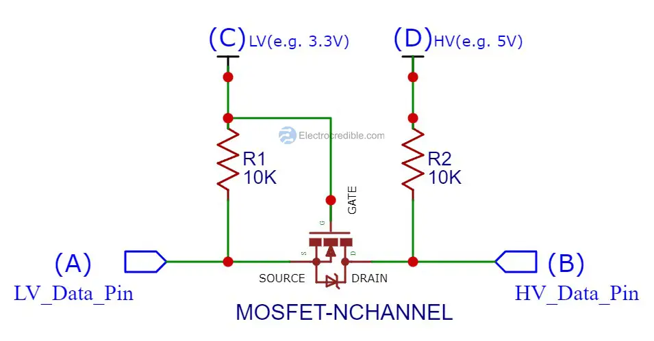
In the logic level shifter circuit shown above, consider that the MOSFET turns on fully when we supply a Gate-Source voltage (VGS) of 3.3V.
Low-level to high-level conversion: When the voltage at point A is at 3.3V, the MOSFET stays in the cut-off region as the voltage difference between the Gate and Source is less than the threshold voltage required for the MOSFET to turn on. The voltage at point B is pulled up to 5V by the R2 resistor. So for 3.3V at point A, we get 5V at point B.
If the voltage at point A is 0V, the ON resistance of the MOSFET decreases due to a voltage difference between the gate and the source. As the MOSFET almost behaves like a short in this condition, point B now becomes 0V. Hence, for 0V at point A, we get 0V at the point.
In this case, the input and output voltage can be related as:
| Input Voltage(node A) | Output Voltage(node B) |
| 3.3 Volt | 5 Volt |
| 0 Volt | 0 Volt |
High-level to low-level conversion: When the voltage at terminal B is at 5V, the MOSFET stays in the cut-off region, and node A is pulled to 3.3V by the pull-up resistor R1. When node B is at 0V, the intrinsic body diode of the MOSFET starts conducting as it gets forward-biased. This pulls the voltage at point A close to 0V. So in this case too, we get the corresponding voltages on the other side.
Now, we can relate the input and output voltage as:
| Input Voltage(node B) | Output Voltage(node A) |
| 5 Volt | 3.3 Volt |
| 0 Volt | 0 Volt |
Thus, the voltages shift as required using this simple n-channel MOSFET circuit.
Demonstration
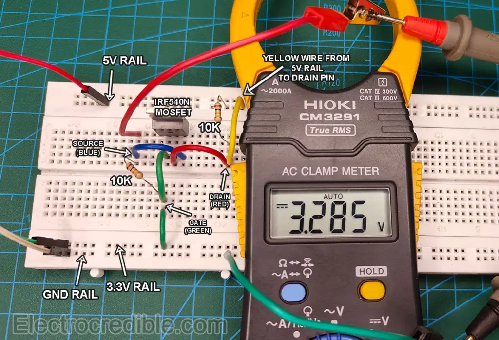
Low to High Level Shifting
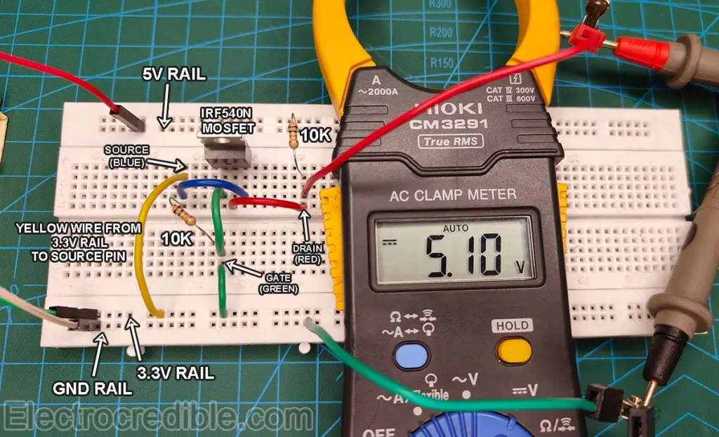
In the circuit shown above, an IRF540N N-Channel MOSFET is used to make a bidirectional logic level converter. The Blue wire is connected to the Source pin, the Red wire to the Drain pin and the Green wire to the Gate pin of the MOSFET.
The multimeter is set to sense the DC voltage on the Drain pin of the MOSFET. Low-level to high-level conversion is demonstrated, so the Source pin is the input while the Drain pin is the output.
When 3.3V is supplied to the Source pin (through the yellow wire), around 5V can be seen on the Drain pin. Similarly, for an input of 0V in the Source pin, we will get 0V in the Drain pin.
High to Low Level Shifting
In high to low level shifting, the Drain pin is the input while the Source pin is the output. When 5V is supplied to the Drain pin (through the yellow wire), around 3.3V can be seen on the Source pin. Similarly, for an input of 0V in the Drain pin, we will get 0V in the Source pin.
Note: The input needs to be shorted to Ground for logical “0” as input, otherwise the output may stay in a floating state. Use a pull-down resistor if required.
Bidirectional Logic Level Converter Breakout Board
The diagram below shows how the components in a logic-level converter breakout board are wired. Note that the GND pins are shorted from one side to another.
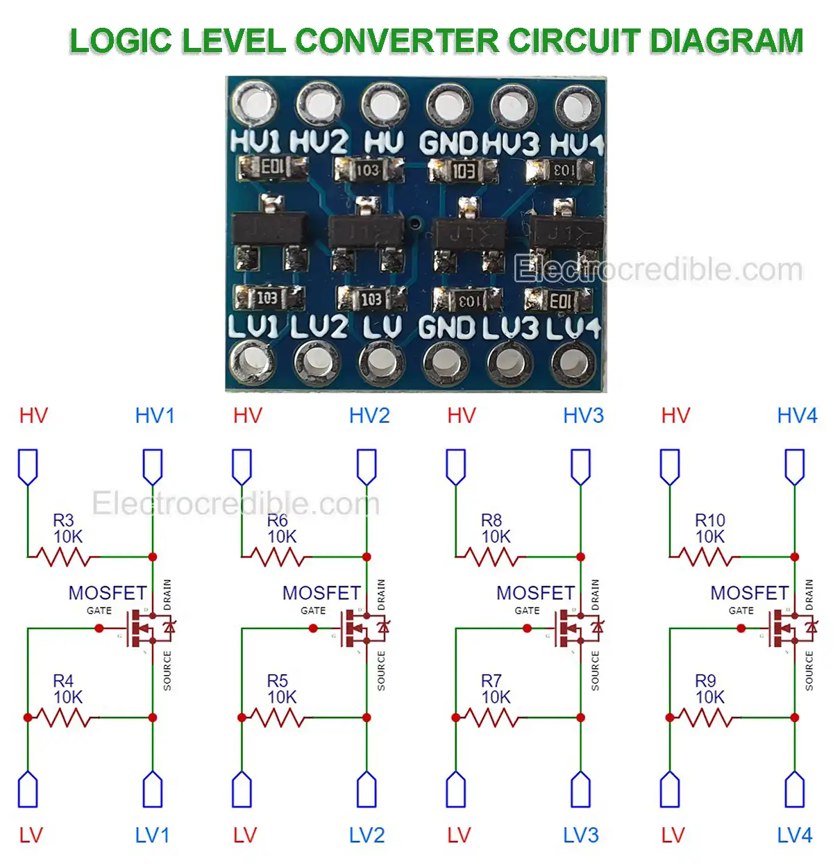
A bidirectional logic-level converter module contains multiple channels with identical circuits as seen earlier. The modules I used have MOSFETs with J1Y marked on them which are commonly used n-channel MOSFETs in an SMD package.
These modules are often used to convert I2C voltage levels when interfacing 3.3V-operated devices with 5V-operated devices. Logic-level shifter modules come in handy when we do not want to deal with discrete components such as transistors or MOSFETs.
Uses of Logic Level Shifter
There are many applications for logic-level converters in electronic circuits such as:
- Bidirectional communication using protocols such as I2C, SPI, and Serial communication between different devices.
- Interfacing chips of different logic families such TTL and CMOS.
- Interfacing of 3.3V compatible sensors with 5V-operated development boards such as Arduino UNO.
Read the examples below to get a better understanding of logic level shifters.
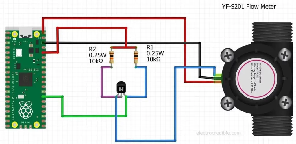
Our article on interfacing flow sensor with Raspberry Pi Pico demonstrates how to use a logic-level converter to interface a 5V compatible sensor to the 3.3V-operated microcontroller RP2040.
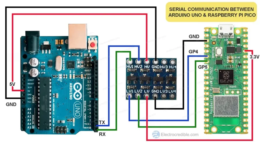
We also have a post that describes how to establish serial communication between Arduino UNO and Raspberry Pi Pico. You can learn more about how the logic level shifter breakout board is used by reading the article.
Summary
In this article, we discussed how to shift logic levels using transistors, MOSFETs, and ready-made breakout board modules. While a single NPN transistor can act as a unidirectional level shifter, a MOSFET can act as a bidirectional logic level converter. A breakout board with multiple level shifting channels is convenient when there are multiple inputs/outputs with different voltage level requirements.
Leave a Reply